MurumLux: Overview
2015-05-12 22:20 by Ian
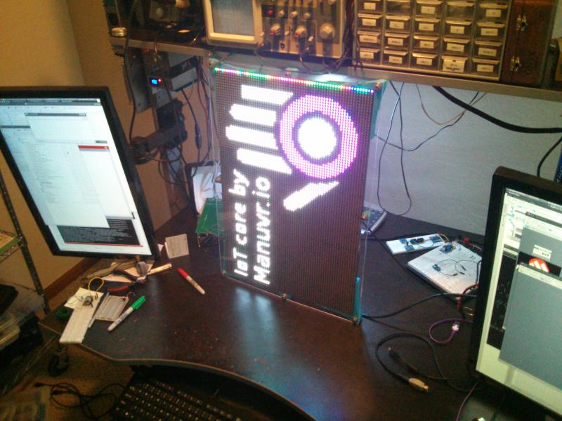
This is a high-level overview of MurumLux (Latin: "Wall of light"). It is a demo piece I built using Microchip's current top-of-the-line microcontroller. The chipKIT team wanted something eye-popping and fun to use for the bay area Maker Faire (May 2015). This is what I rolled for them.
The design criteria specified that it be interactive and sturdy. The MGC3130 (also a Microchip part) was offered as a possible sensor for user interaction. My write up on it is located here. "Sturdy" was left to my best technical judgement.
Is it possible?
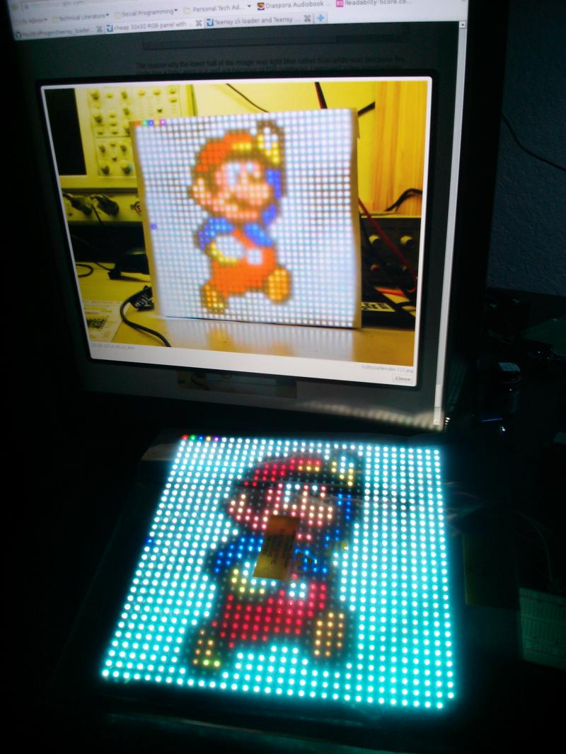
The real wildcard in my mind was the panels themselves. So I ordered a few from Adafruit and got this demo code up on a Teensy3. I then proceeded to measure timings and tolerances.
For this kind of display, the frame-rate needs to be ridiculously high to get any sense of color, so I wanted to see what I would be dealing with. A few hours of tinkering, and I decided it would work.
Step 2: Choose parts, and plan high-level organization
Here is the critical parts list:
- 6 32x32 6mm pitch RGB LED matrices (Panel)
- 1 PIC32MZ via the Digilent ChipKIT WiFire board (Panel)
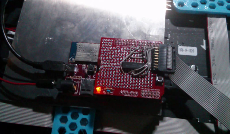
- 1 UNO32 prototyping shield (Panel)
- 1 74HCT174 hex D-flipflop (Panel)
- 1 200w PSU @5v (Panel)
- 2 IPLogika iPACK401 Ethernet modules (Both units)
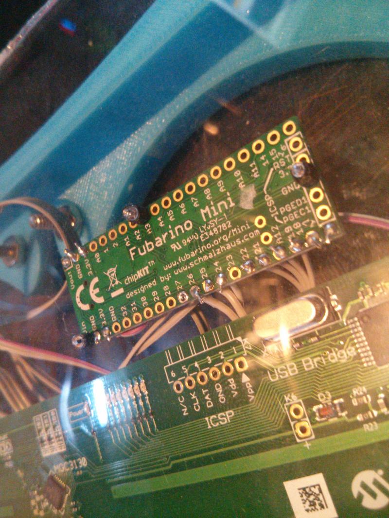
- 1 Fubarino Mini (E-Field box)
- 1 Sabrewing MGC3130 Development Kit (E-Field box)
The WiFire board was chosen because it was built with Microchip's current top-of-the-line microcontroler. At 200MHz with a double-wide FPU(!), it is easily the most computer I've ever used in a TQPF package. More about the PIC32MZ later...
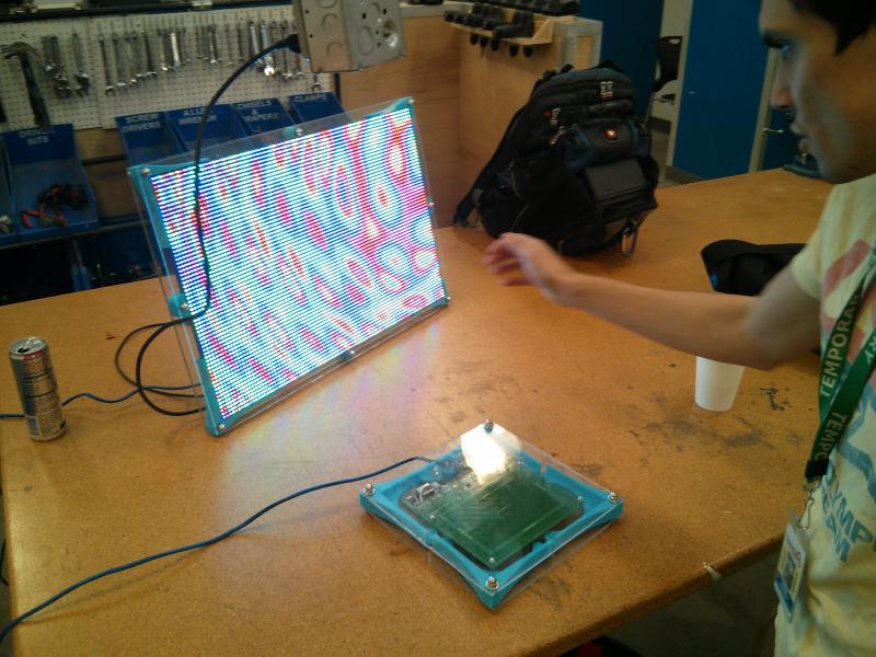
The LED panels were chosen because: eye-popping. No joke... these things are bright. If you look again at the image above, notice that I've attenuated the panel with a mylar anti-static bag. I spent 2 weeks at my workbench writing code while wearing sunglasses at 1am.
I was enthusiastic about Microchip's suggestion that I use the MGC3130. I'm dealing with the idea of "gesture" already in Digitabulum, and another approach to the idea seemed worthwhile. So that choice was easy. The worst problem was How to get i2c to travel 3 meters?
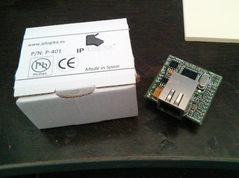
The answer to that ended up coming from a Spanish company named IPLogika that makes an Ethernet shield for small microcontrollers. Ethernet was chosen to be the link between the E-field box and the main panel because it was designed for the sort of distances we are talking about (the cable is ~3 meters) and it allows power to be supplied via PoE. As it turns out, the fact that the module has built in TCP server/client functionality was a tremendous debugging aid. My write-up on their part is located here.
The IPLogika board can't be expected to talk to the i2c board for me. Or maybe it can. I don't know. This part is brand new and there wasn't much documentation on it. But I assumed I would need another microcontroller in the e-field box to make the bridge. Microchip came though again with a spiffy little gum-stick board: The Fubarino Mini.
Step 3: Build a durable panel
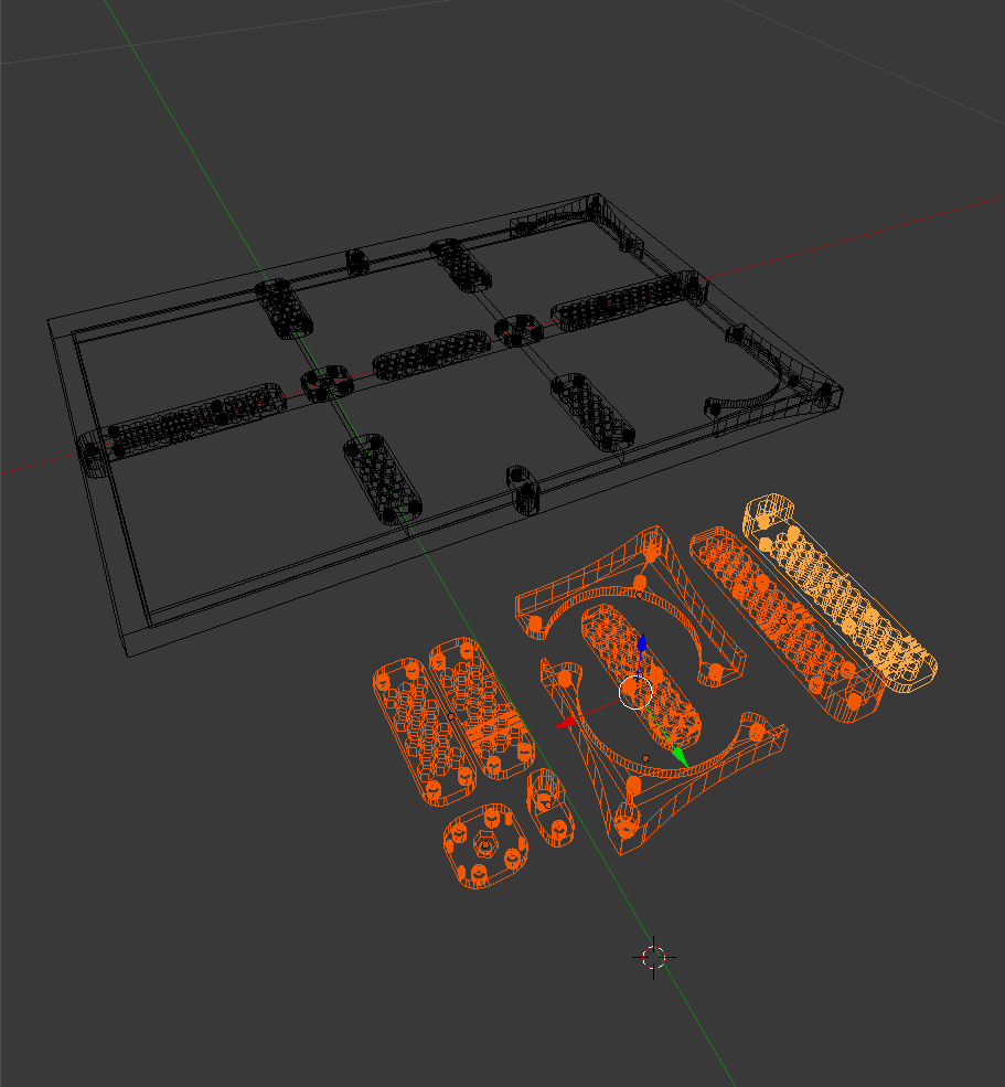
Take dimensions... Blender...
Here is my mechanical model of the panel, and the resulting unique part set (highlighted).
And another in ortho...
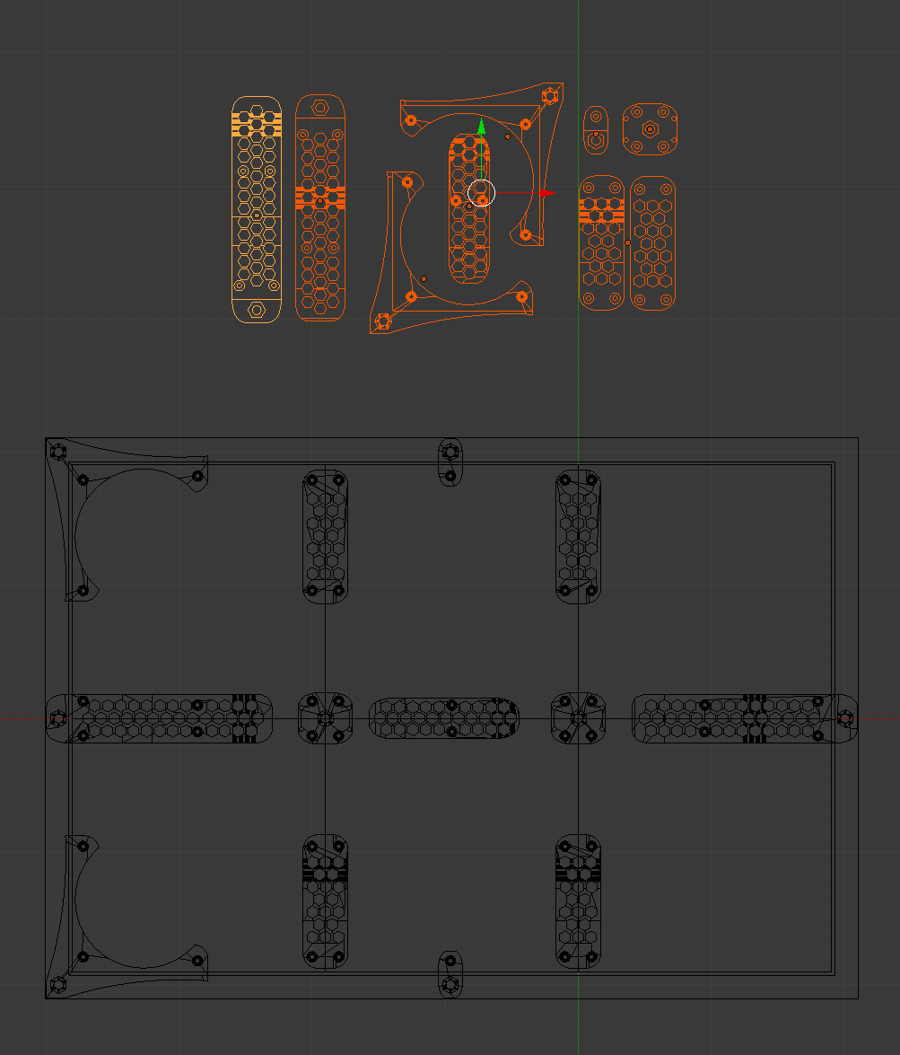
The model instantiated:
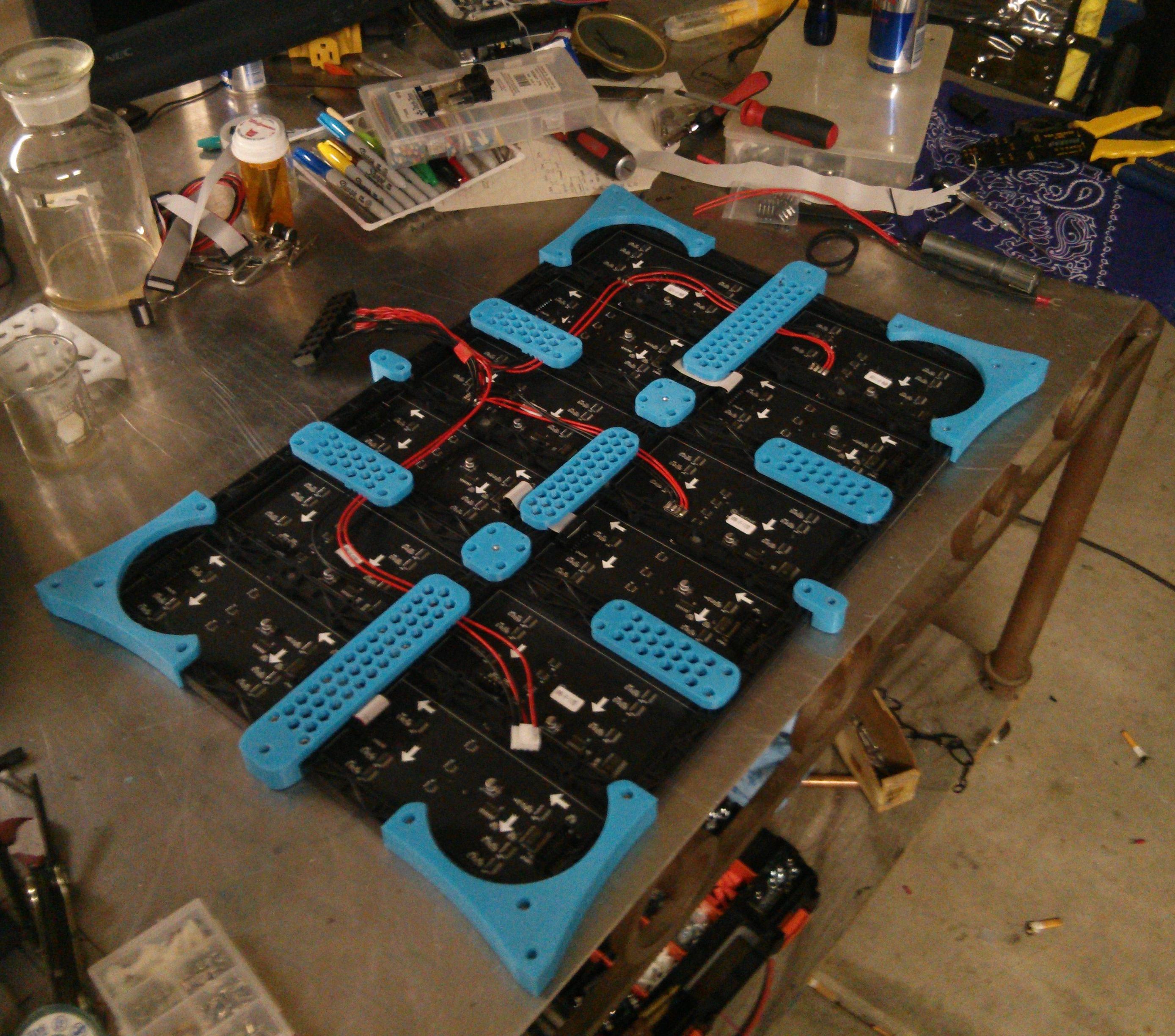
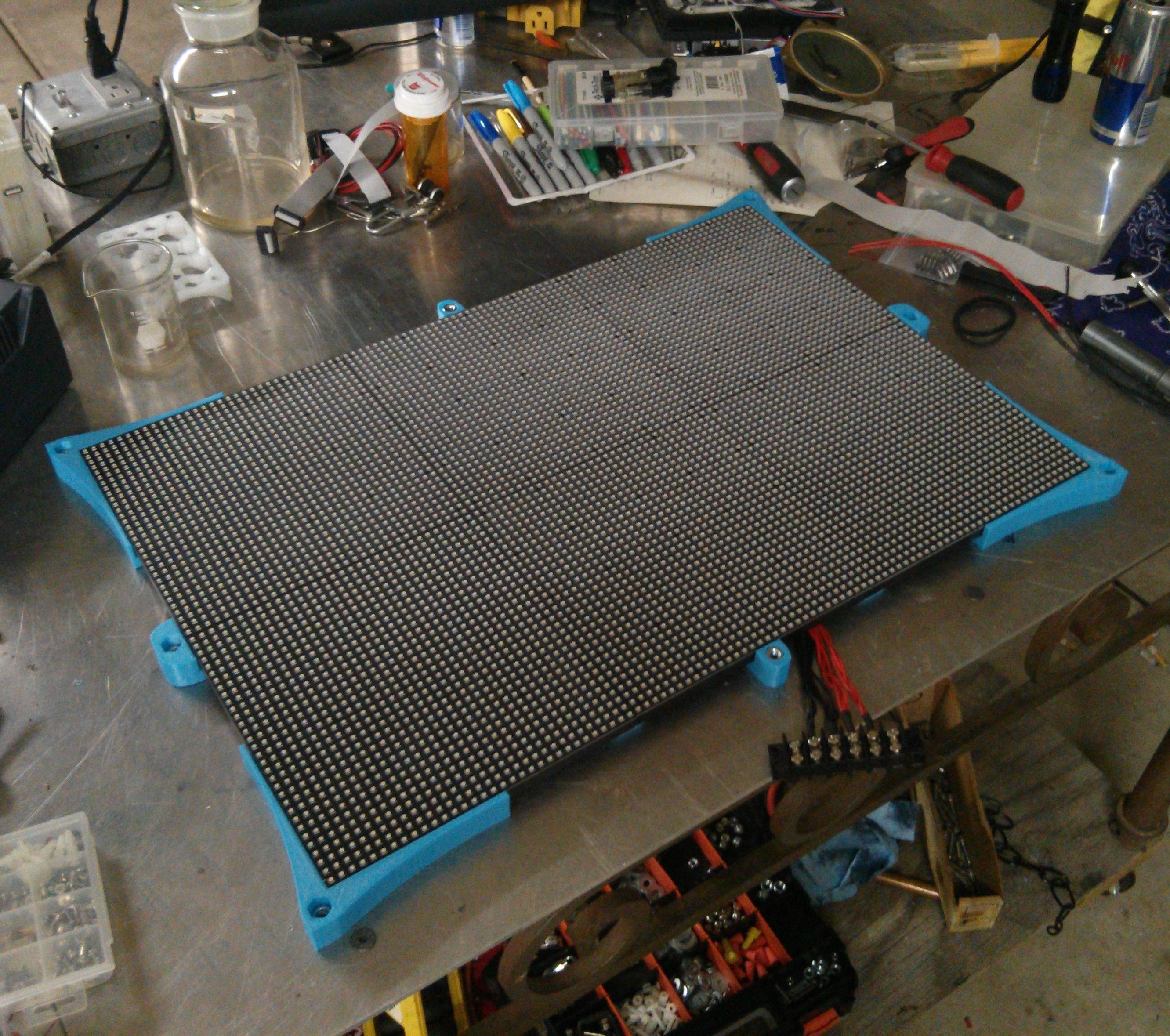
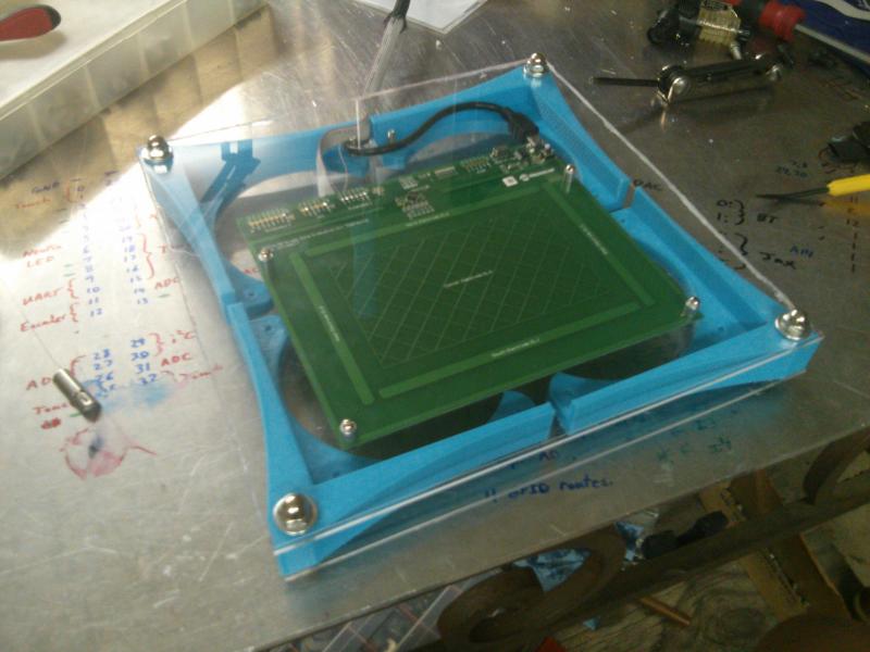
The rear 1/4" acrylic panel, all drilled, and with parts mounted. You can see the large aluminum plate that holds the PSU and VESA mount.
I build all of my non-trivial project enclosures this way now. And this is why: My Blender model told me that the resulting assembled unit ought to be 16.5" wide....

I previously did some show-and-tell on YouTube regarding the 3D modelling and printing techniques that I employed as part of a 3D printer wizardry series.
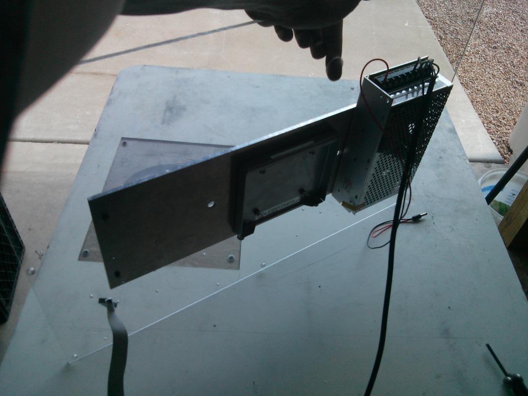
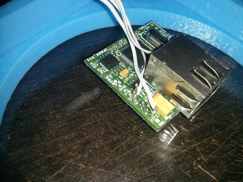
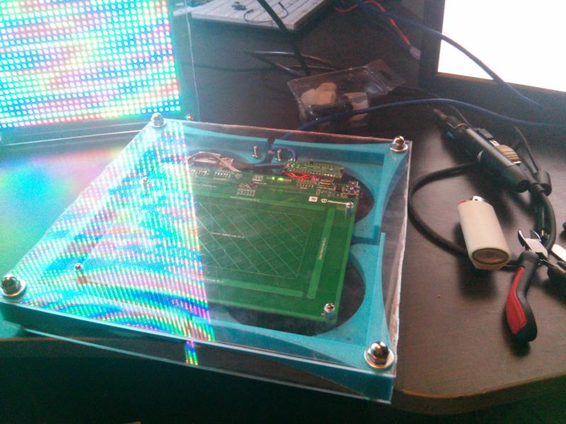
And here we have the basic build of the E-field box:
Now... need to press-fit those parts that don't have mounting holes... Let's do the Ethernet module first....
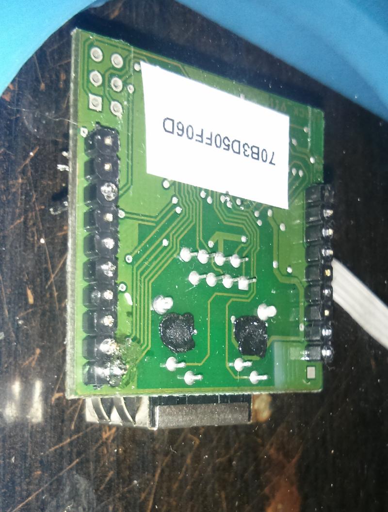
Here is a shot of the back-side of that mounting job, for clarity. When parts don't have mounting holes, I often resort to these sorts of tricks. In this case, I've cut off all the pins, and used a hot soldering iron to press the remains of the pins through the PCB, and let the hot pin sink into the acrylic. Here I did 12 pins. On the Fubarino I only did 3.
Now the Fubarino. Imma flip it upside down to show it off a bit...
Here is the completed e-field box basking in triple-peak radiation.
Meet my durability tester. He approved the build for use by random people at a trade-show.
Step 4: Program the thing
My general approach throughout this project has been: throw bandwidth and memory at the problem. This is the bottleneck I've often run into on the STM32F4, and I wanted to evaluate the PIC32MZ as a replacement for Digitabulum. So I'm going to make it bleed....
Quick facts:
- The panels have 4 address lines
- The panels take 6-bits of parallel data which is driven in by a clock signal
- The panels are designed to be chained together
- Chaining panels lowers the maximum frame-rate
When I set out to make the interface to the LED panel, I figured I would drive them in 2 chains of 3 panels (there are 6 total) via the PMP port operating in 16-bit mode. I would use the remaining 4 bits to inform the demultiplexers in the panels which row I was updating. All this while driving the panel's clock signal with a chip-select pin. Net effect? No memory waste, maximum comprehensibility of the render buffer's layout, and I can run DMA in a continuous loop to allow my software to ignore the panel completely.
That is what I wanted to do.
It was not done that way because of the inaccessibility of the PMP control signals on the board I was using. Not surprising, because using the PMP port is probably not a common use-case for this sort of board. So I threw bandwidth and memory at the problem, and baked two clock signals into the byte stream I would send to the panel over an 8-bit PORTE DMA transfer. One clock signal is for the panel's data, and the other is for the 74HCT174 I bolted onto the protoshield that Microchip so generously provided:
But since I'm now sending my clock signals in the data stream, I have to send twice as much data. It also means I am obliged to include control signal information in that stream. It doubles the size of the frame buffer, and quarters my effective frame-rate (because moving twice the data at half the width). But after reading the PIC32MZ specs, and knowing that the program wasn't going to be using much memory bandwidth anyhow...

Deeper details can be found by reading the doc in the frame buffer init fxn.
This concession limited my frame update period to about 1470 microseconds +/- 3us. That works out to be about 680 frames per second. While this might seem ample, we have to PWM the color. Which means that if we want (suppose) 24-bit color (8-bits per channel), we need to render 256 frames to get a single frame at that color depth. So if I wanted 24-bit color at 30fps using such a display, I would need to render at (256 * 30 = 7680) fps. So the deepest color I could manage would be 9-bit under these conditions. All that aside, my frame buffer is TWICE the size it needs to be. Which means that the PIC32MZ DMA peripheral is moving one byte every 236ns, in blocks of ~50KB in a continuous loop with zero software intervention. That's 4.243MB/sec over GPIO. I'm certain PMP would be faster.
Even if the rate isn't intrinsically faster, if I bust out the microscope and solder to that inaccessible strobe pin, the PIC32MZ has more than enough bandwidth to push the panel at 24-bit color. And since DMA is driving the whole process, the CPU is free to do trigonometry in its (quite plush) FPU unhindered, since that task uses very little memory bandwidth. Re-rendering Adafruit's coherent noise algorithm completes much faster than the DMA takes to move the frame. So I can effectively render a fresh frame of coherent noise at least 680 times per second. This reflects a monstrous quantity of FPU work. I also suspect (but have not yet verified) that the PIC32MZ's FPU handles the modulus operation, whereas the FPU in the STM32F4 does not. I am quite impressed.
The flash memory in the PIC32MZ also seems to be inherently faster than the flash in the STM32F4 from what I can tell. I never experienced a CPU stall (from what I could tell) waiting for flash access. So the effort Microchip put into those subsystems has paid off.
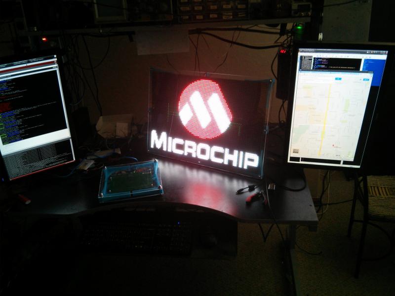
Here are some of the logos the panel renders during inactivity...
Video playlist:
Previous: WebRemote Relocation
Next: Arduino library for the MGC3130